- 您现在的位置:买卖IC网 > Sheet目录1997 > ICS8430S07AKILF (IDT, Integrated Device Technology Inc)IC CLK GENERATOR PLL 32VFQFN
ICS8430S07AKI REVISION A SEPTEMBER 3, 2009
18
2009 Integrated Device Technology, Inc.
ICS8430S07I Data Sheet
CLOCK GENERATOR FOR CAVIUM PROCESSORS
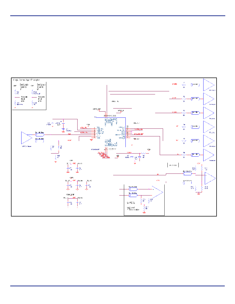
Application Schematic
Figure 8 shows a schematic example of using an ICS8430S07I. The
crystal inputs are parallel resonant crystal with load capacitor
CL=18pF. The frequency fine tuning capacitors C1 and C2 are
optional. The tuning capacitor value can be slightly adjusted to
optimize the frequency accuracy. This schematic example shows
hardwired logic control input handling. The logic inputs can also be
driven by 3.3V LVCMOS drivers. It is recommended to have one
bypass capacitor per power pin. In general, the bypass capacitor
values are ranged from 0.01uF to 0.1uF. Each bypass capacitor
should be located as close as possible to the power pin. The low pass
filter R6, C3 and C4 for clean analog supply should also be located
as close to the VDDA pin as possible. Only two examples of LVPECL
termination and one example of LVCMOS termination are shown in
this schematic. Additional examples of LVPECL terminations and
LVCMOS terminations can be found in the LVPECL Termination and
LVCMOS Termination Application Notes.
Figure 8. ICS8430S07I Schematic Example
发布紧急采购,3分钟左右您将得到回复。
相关PDF资料
ICS8430S10BYI-02LF
IC CLK GENERATOR PLL 48TQFP
ICS84314AY-02LFT
IC SYNTHESIZER 700MHZ 32-LQFP
ICS843156AKILF
IC CLK GENERATOR 32VFQFP
ICS843156AKLF
IC CLK GENERATOR 32VFQFP
ICS843202AYILF
IC SYNTHESIZER 680MHZ 32-LQFP
ICS843204AGILF
IC SYNTHESIZER LVPECL 48-TSSOP
ICS84320AY-01LN
IC SYNTHESIZER GP LVPECL 32-LQFP
ICS84320AYI-01LF
IC FREQ SYNTHESIZER 32TQFP
相关代理商/技术参数
ICS8430S07AKILFT
功能描述:IC CLK GENERATOR PLL 32VFQFN RoHS:是 类别:集成电路 (IC) >> 时钟/计时 - 专用 系列:- 标准包装:1,500 系列:- 类型:时钟缓冲器/驱动器 PLL:是 主要目的:- 输入:- 输出:- 电路数:- 比率 - 输入:输出:- 差分 - 输入:输出:- 频率 - 最大:- 电源电压:3.3V 工作温度:0°C ~ 70°C 安装类型:表面贴装 封装/外壳:28-SSOP(0.209",5.30mm 宽) 供应商设备封装:28-SSOP 包装:带卷 (TR) 其它名称:93786AFT
ICS8430S07I
制造商:IDT 制造商全称:Integrated Device Technology 功能描述:Clock Generator for Cavium Processors
ICS8430S10AYILF
功能描述:IC CLK GENERATOR PLL 48TQFP RoHS:是 类别:集成电路 (IC) >> 时钟/计时 - 专用 系列:- 标准包装:1,500 系列:- 类型:时钟缓冲器/驱动器 PLL:是 主要目的:- 输入:- 输出:- 电路数:- 比率 - 输入:输出:- 差分 - 输入:输出:- 频率 - 最大:- 电源电压:3.3V 工作温度:0°C ~ 70°C 安装类型:表面贴装 封装/外壳:28-SSOP(0.209",5.30mm 宽) 供应商设备封装:28-SSOP 包装:带卷 (TR) 其它名称:93786AFT
ICS8430S10AYILFT
功能描述:IC CLK GENERATOR PLL 48TQFP RoHS:是 类别:集成电路 (IC) >> 时钟/计时 - 专用 系列:- 标准包装:1,500 系列:- 类型:时钟缓冲器/驱动器 PLL:是 主要目的:- 输入:- 输出:- 电路数:- 比率 - 输入:输出:- 差分 - 输入:输出:- 频率 - 最大:- 电源电压:3.3V 工作温度:0°C ~ 70°C 安装类型:表面贴装 封装/外壳:28-SSOP(0.209",5.30mm 宽) 供应商设备封装:28-SSOP 包装:带卷 (TR) 其它名称:93786AFT
ICS8430S10BYI-02LF
功能描述:IC CLK GENERATOR PLL 48TQFP RoHS:是 类别:集成电路 (IC) >> 时钟/计时 - 专用 系列:- 标准包装:1,500 系列:- 类型:时钟缓冲器/驱动器 PLL:是 主要目的:- 输入:- 输出:- 电路数:- 比率 - 输入:输出:- 差分 - 输入:输出:- 频率 - 最大:- 电源电压:3.3V 工作温度:0°C ~ 70°C 安装类型:表面贴装 封装/外壳:28-SSOP(0.209",5.30mm 宽) 供应商设备封装:28-SSOP 包装:带卷 (TR) 其它名称:93786AFT
ICS8430S10BYI-02LFT
功能描述:IC CLK GENERATOR PLL 48TQFP RoHS:是 类别:集成电路 (IC) >> 时钟/计时 - 专用 系列:- 标准包装:1,500 系列:- 类型:时钟缓冲器/驱动器 PLL:是 主要目的:- 输入:- 输出:- 电路数:- 比率 - 输入:输出:- 差分 - 输入:输出:- 频率 - 最大:- 电源电压:3.3V 工作温度:0°C ~ 70°C 安装类型:表面贴装 封装/外壳:28-SSOP(0.209",5.30mm 宽) 供应商设备封装:28-SSOP 包装:带卷 (TR) 其它名称:93786AFT
ICS8430S10I-03
制造商:IDT 制造商全称:Integrated Device Technology 功能描述:Clock Generator for Cavium Processors
ICS8431-01
制造商:ICS 制造商全称:ICS 功能描述:200MHZ, LOW JITTER, LVPECL FREQUENCY SYNTHESIZER